How to Make Your Own Printed Circuit Board
A printed circuit board will make your electrical circuits much better. You won’t have to spend time joining multiple wires and getting loose components. All you need to do is to place your elements on the board and solder them to the board. It will also make your work much better and organized than a breadboard.
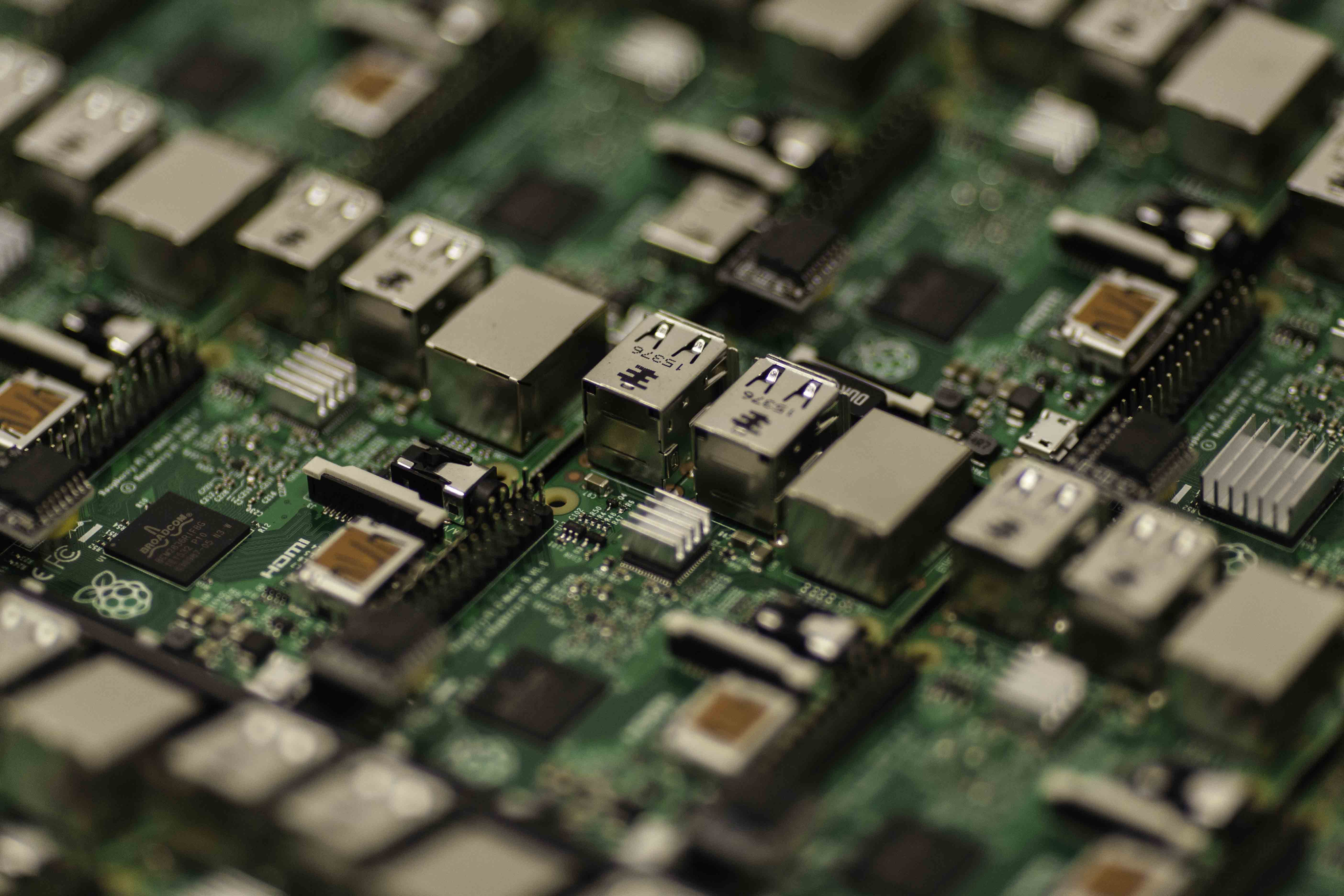
A printed circuit board connects electronic components electrically by using conductive pads, tracks, and other features that are etched from copper boards laminated onto a substrate.
The various ways of making printed circuit boards are the etching method, fab house method, and milling method. The etching is the most commonly used method for DIY purposes, and it is the method that will be explained in this article.
1. Design your board:
Firstly, you have to design your PCB on a computer using any of the various PCB layout software available. Some of the software are free, while some will require you to buy a license.
They are easy to use for simple designs. But for more complex boards, you can run a simple Google search on ‘how to make a PCB with an unusual shape or size.’
2. Print the layout:
The next step to take is to print the board layout that you have designed on a sheet of transparent paper. You can also use a Propalcote paper.
3. Cut the copper board:
Cut out the copper board that you will use. The board you cut out should be slightly larger than the paper printout so that it can accommodate it.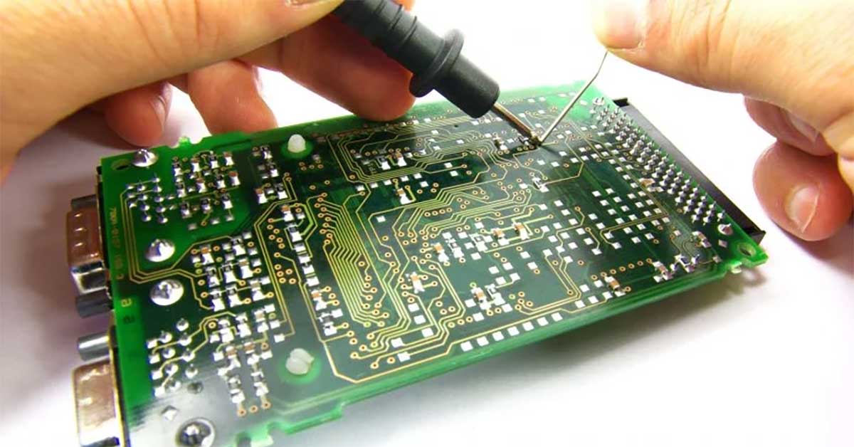
4. Clean the copper board:
The next step to take is to clean the board. Use a metal sponge or other effective materials to clean the board. This will remove the photoresist layer of the copper board and the top oxide layer of the copper board. This will also make the image from the paper stick to the board better.
5. Transfer the layout:
The next step to take is to cut off the printout and transfer the layout to the board. Use tape to hold the paper to the board.
6. Iron the board:
The next thing to do is to iron the copper board. You can set the electric iron to the maximum setting and then press the board for about eight minutes or so. Press all over and around the edges.
Apply a lot of pressure and be thorough with your ironing. The ink from the paper will be transferred to the copper plate due to the heat.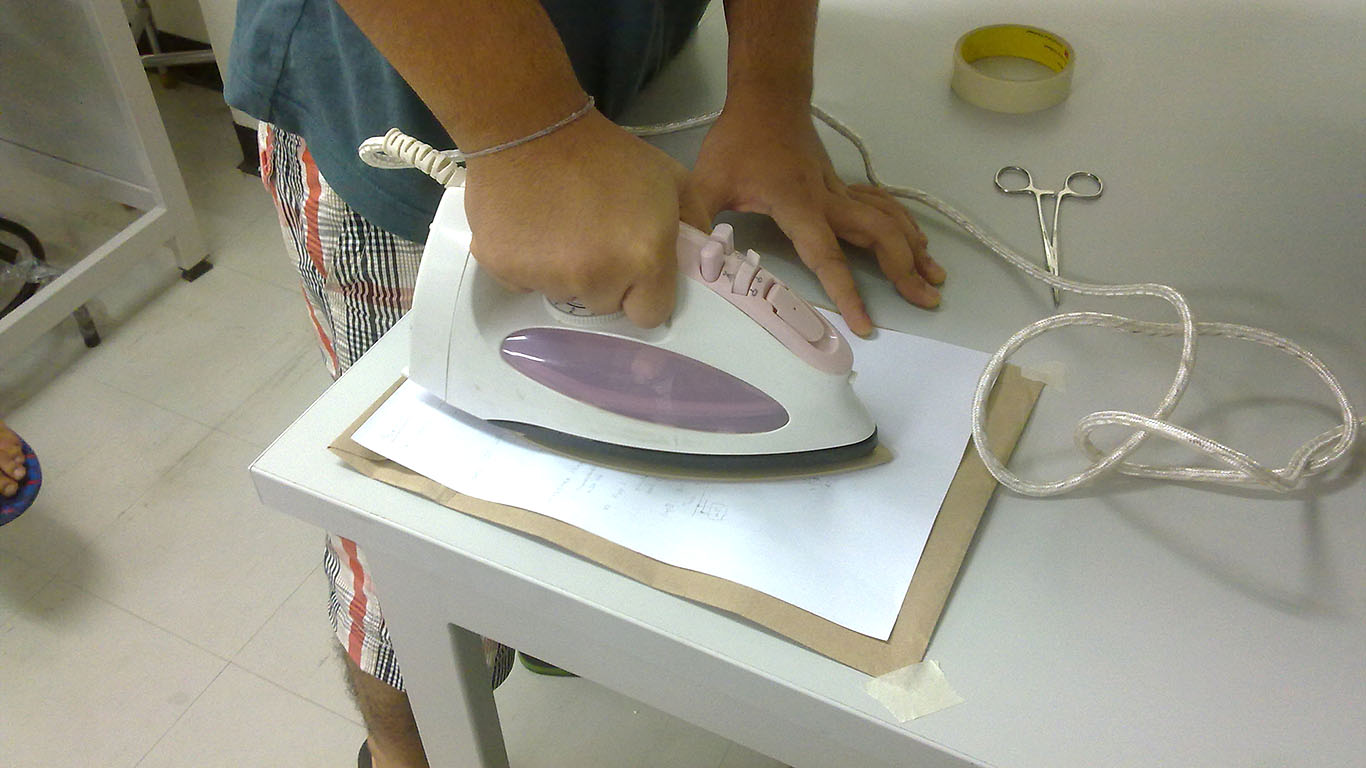
7. Brush the board:
After ironing the board, transfer it to water and remove the paper. Be careful while dealing with the board, as it will be very hot due to the effect of the iron. Also, be careful while removing the paper. Do it gently. For tracks that are faint, you can use a black marker to darken them.
8. Transfer the board to an etching solution:
The next step to take is to transfer the board to an etching solution. You should use a pair of gloves to avoid the solution coming into contact with your skin. You can prepare an etching solution by mixing about two to three teaspoons of FeCl3 or Ferric Chloride powder into water. The solution will react with the copper and remove unwanted copper from the printed circuit board. Once all the tracks are well defined, remove the board. This will take about 30 minutes. If you remove the board and see that it has not been etched properly, put it back into the solution.
9. Use acetone to clean the board:
The next thing to do is to clean the board with a thinner like acetone. This will scrub away the plastic laser toner.
10. Drill the holes:
After cleaning the board with acetone, you need to drill the solder holes on the board. Do not make the holes too big or too small. Just make them adequate to fit in your components. 
Conclusion
If you want that green look that some industrial printed circuit board has, you can add paint that is resistant to solder to the board. If you want something more creative like unusual PCB shapes and sizes, you can check online blogs for ‘how to make a PCB with an unusual shape or size.’